- 您现在的位置:买卖IC网 > Sheet目录1214 > EVAL-ADE7753ZEB (Analog Devices Inc)BOARD EVALUATION AD7753
�� ��
��
��ADE7753�
�TIMING� CHARACTERISTICS�
�AV� DD� =� DV� DD� =� 5� V� ±� 5%,� AGND� =� DGND� =� 0� V,� on-chip� reference,� CLKIN� =� 3.579545� MHz� XTAL,� T� MIN� to� T� MAX� =� ?40°C� to� +85°C.�
�Sample� tested� during� initial� release� and� after� any� redesign� or� process� change� that� could� affect� this� parameter.� All� input� signals� are� specified� with�
�tr� =� tf� =� 5� ns� (10%� to� 90%)� and� timed� from� a� voltage� level� of� 1.6� V.� See� Figure� 3,� Figure� 4,� and� the� ADE7753� Serial� Interface� section.�
�Table� 2.�
�Parameter�
�Spec�
�Unit�
�Test� Conditions/Comments�
�Write� Timing�
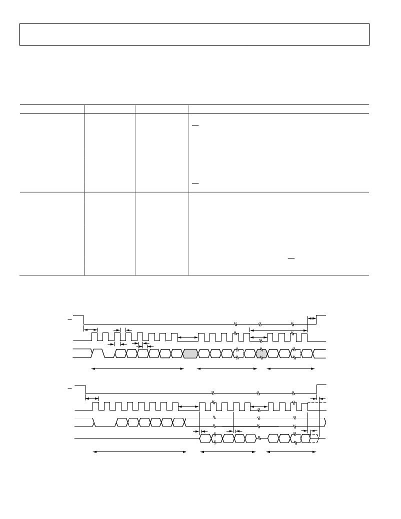
�t� 1�
�t� 2�
�t� 3�
�t� 4�
�t� 5�
�t� 6�
�t� 7�
�t� 8�
�50�
�50�
�50�
�10�
�5�
�4�
�50�
�100�
�ns� (min)�
�ns� (min)�
�ns� (min)�
�ns� (min)�
�ns� (min)�
�μs� (min)�
�ns� (min)�
�ns� (min)�
�CS� falling� edge� to� first� SCLK� falling� edge.�
�SCLK� logic� high� pulse� width.�
�SCLK� logic� low� pulse� width.�
�Valid� data� setup� time� before� falling� edge� of� SCLK.�
�Data� hold� time� after� SCLK� falling� edge.�
�Minimum� time� between� the� end� of� data� byte� transfers.�
�Minimum� time� between� byte� transfers� during� a� serial� write.�
�CS� hold� time� after� SCLK� falling� edge.�
�Read� Timing�
��4�
�μs� (min)�
�Minimum� time� between� read� command� (i.e.,� a� write� to� communication�
�register)� and� data� read.�
�t� 10�
�t� 11�
�50�
�30�
�ns� (min)�
�ns� (min)�
�Minimum� time� between� data� byte� transfers� during� a� multibyte� read.�
�Data� access� time� after� SCLK� rising� edge� following� a� write� to� the�
�communications� register.�
���100�
�10�
�100�
�10�
�ns� (max)�
�ns� (min)�
�ns� (max)�
�ns� (min)�
�Bus� relinquish� time� after� falling� edge� of� SCLK.�
�Bus� relinquish� time� after� rising� edge� of� CS.�
�1�
�2�
�3�
�Minimum� time� between� read� command� and� data� read� for� all� registers� except� waveform� register,� which� is� t� 9� =� 500� ns� min.�
�Measured� with� the� load� circuit� in� Figure� 2� and� defined� as� the� time� required� for� the� output� to� cross� 0.8� V� or� 2.4� V.�
�Derived� from� the� measured� time� taken� by� the� data� outputs� to� change� 0.5� V� when� loaded� with� the� circuit� in� Figure� 2.� The� measured� number� is� then� extrapolated� back�
�to� remove� the� effects� of� charging� or� discharging� the� 50� pF� capacitor.� This� means� that� the� time� quoted� in� the� timing� characteristics� is� the� true� bus� relinquish� time� of�
�the� part� and� is� independent� of� the� bus� loading.�
�t� 8�
�CS�
�SCLK�
�t� 1�
�t� 3�
�t� 7�
�t� 7�
�t� 6�
�t� 2�
�t� 4�
�t� 5�
�DIN�
�1�
�0�
�A5�
�A4�
�A3�
�A2�
�A1�
�A0�
�DB7�
�DB0�
�DB7�
�DB0�
�COMMAND� BYTE�
�MOST� SIGNIFICANT� BYTE�
�LEAST� SIGNIFICANT� BYTE�
�02875-0-081�
�Figure� 3.� Serial� Write� Timing�
�CS�
�t� 1�
�t� 13�
�SCLK�
�t� 9�
�t� 10�
�DIN�
�0�
�0�
�A5�
�A4�
�A3�
�A2�
�A1�
�A0�
�t� 11�
�t� 11�
�t� 12�
�DOUT�
�DB7�
�DB0�
�DB7�
�DB0�
�COMMAND� BYTE�
�MOST� SIGNIFICANT� BYTE�
�LEAST� SIGNIFICANT� BYTE�
�02875-0-083�
�Figure� 4.� Serial� Read� Timing�
�Rev.� C� |� Page� 6� of� 60�
�发布紧急采购,3分钟左右您将得到回复。
相关PDF资料
EVAL-ADE7754EBZ
BOARD EVALAUTION FOR ADE7754
EVAL-ADE7755ZEB
BOARD EVALUATION FOR AD7755
EVAL-ADE7758ZEB
BOARD EVAL FOR AD7758
EVAL-ADE7759EBZ
BOARD EVALUATION FOR ADE7759
EVAL-ADE7762EBZ
BOARD EVALUATION FOR ADE7762
EVAL-ADE7763ZEB
BOARD EVALUATION FOR ADE7763
EVAL-ADE7816EBZ
BOARD EVALUATION FOR ADE7816
EVAL-ADE7878EBZ
BOARD EVAL FOR ADE7878
相关代理商/技术参数
EVAL-ADE7754EB
制造商:Analog Devices 功能描述:EVALUATION BOARD FOR POWER METERING, POLYPHASE MULTIFUNCTION ENERGY METERING IC WITH SERIAL PORT 制造商:Analog Devices 功能描述:PWR METERING, POLYPHASE MULTIFUNCTION ENERGY METERING IC W/ - Bulk
EVAL-ADE7754EBZ
功能描述:BOARD EVALAUTION FOR ADE7754 RoHS:是 类别:编程器,开发系统 >> 评估演示板和套件 系列:- 标准包装:1 系列:- 主要目的:电信,线路接口单元(LIU) 嵌入式:- 已用 IC / 零件:IDT82V2081 主要属性:T1/J1/E1 LIU 次要属性:- 已供物品:板,电源,线缆,CD 其它名称:82EBV2081
EVAL-ADE7755EB
制造商:Analog Devices 功能描述:EVAL BOARD ENERGY METERINGW/PULSE OUTPUT - Bulk
EVAL-ADE7755EBZ
制造商:AD 制造商全称:Analog Devices 功能描述:Energy Metering IC with Pulse Output
EVAL-ADE7755EBZ1
制造商:AD 制造商全称:Analog Devices 功能描述:Energy Metering IC with Pulse Output
EVAL-ADE7755ZEB
功能描述:BOARD EVALUATION FOR AD7755 RoHS:是 类别:编程器,开发系统 >> 评估演示板和套件 系列:- 标准包装:1 系列:- 主要目的:电信,线路接口单元(LIU) 嵌入式:- 已用 IC / 零件:IDT82V2081 主要属性:T1/J1/E1 LIU 次要属性:- 已供物品:板,电源,线缆,CD 其它名称:82EBV2081
EVAL-ADE7756EB
制造商:Analog Devices 功能描述:EVAL BD DOCUMENTATION ADE7756 ENERGY METERING IC - Bulk 制造商:Rochester Electronics LLC 功能描述:
EVAL-ADE7757AEBZ
制造商:Analog Devices 功能描述:EVALUATION BOARDS - Bulk